
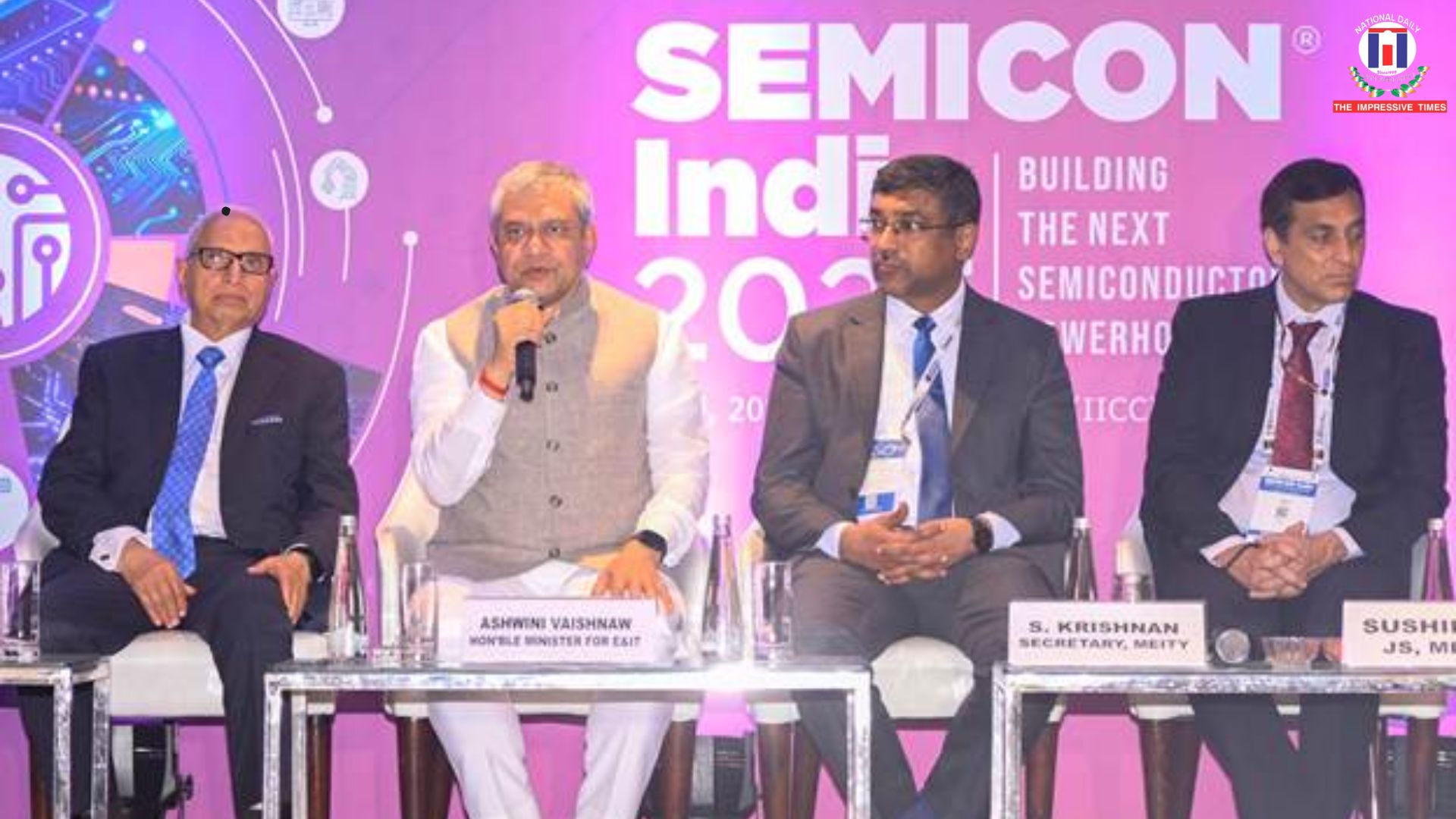
The Union Cabinet has approved Semicon 2.0, a Rs 1,27,500 crore programme that dramatically expands India's semiconductor ambitions. Alongside the Rs 62,500 crore Mobile Phone Manufacturing Scheme, the total outlay of Rs 1.9 lakh crore represents India's most aggressive push yet into electronics manufacturing.
The move builds on the India Semiconductor Mission 1.0, which attracted Rs 1.64 lakh crore in cumulative investments and brought India its first silicon fab, silicon carbide fab, and multiple packaging units.
What You Need to Know
- Semicon 2.0 allocates Rs 1.27 lakh crore across design, fabrication, packaging, materials, equipment, and talent
- The government will take equity stakes in semiconductor startups instead of offering one-time grants
- India targets $500 billion in electronics production by 2030-31
- Three commercial units are already running under ISM 1.0, including Micron's Sanand plant
1. Chip Design and Intellectual Property
India already employs a large pool of semiconductor design engineers working for global companies. Semicon 2.0 aims to convert that expertise into indigenous chip design. Financial support will be available for Indian startups and companies designing chips for strategic and commercial sectors. The programme moves beyond grant-only support by introducing equity co-investment for startups and royalty financing for larger firms.
2. Fabrication and Advanced Packaging
While ISM 1.0 focused primarily on attracting fabrication investments, Semicon 2.0 also targets Outsourced Semiconductor Assembly and Test and Assembly, Testing, Marking and Packaging infrastructure. These segments require lower investment than fabs and can be developed more quickly, allowing India to integrate into global supply chains faster. The Tata fab at Dholera is under construction for commissioning in 2028, and Tata's ATMP plant in Assam covers 171 acres.
3. Equipment and Materials Manufacturing
A critical new pillar supports the manufacturing of semiconductor equipment, specialty materials, chemicals, and industrial gases. India currently has limited presence in these upstream segments. Developing them reduces import dependence and strengthens supply chain resilience. The scheme covers 150 to 500 material categories for both domestic consumption and export.
4. Research and Development
Semicon 2.0 targets a path from India's current 28-110 nm node capability toward 7-3 nm, alongside investments in silicon photonics and advanced packaging technologies. Partnerships have been signed with the United States, European Union, Japan, Singapore, the Netherlands, and Germany to accelerate technology transfer.
5. Talent Development
The programme sets a target of one lakh design engineers within five years, plus operators, engineers, and PhDs for fabrication, packaging, equipment, and materials. This addresses a critical bottleneck: India's engineering talent has historically been concentrated in software, not hardware.
6. Mobile Phone Manufacturing Scheme
Running alongside Semicon 2.0, the MPMS offers sales-linked incentives of 2.25 to 5 percent, with Indian brands receiving the top rate. Additional incentives of up to 1.5 percent apply for domestic sourcing of components, and 3 percent extra for design and R&D by Indian brands. The government expects cumulative production of about Rs 39 lakh crore and 60,000 direct jobs over five years.
Bottom Line
Semicon 2.0 represents India's most comprehensive industrial policy for electronics. By supporting every stage from design to talent to manufacturing, it aims to transform India from an assembler of imported components into a genuine semiconductor powerhouse.